Distortion of Doom (for Bass)


|
This post was updated on .
That one i got on instructables.com, sems a simple one to start modding, specially for the bassists here.
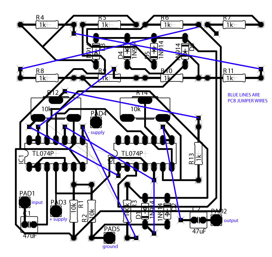 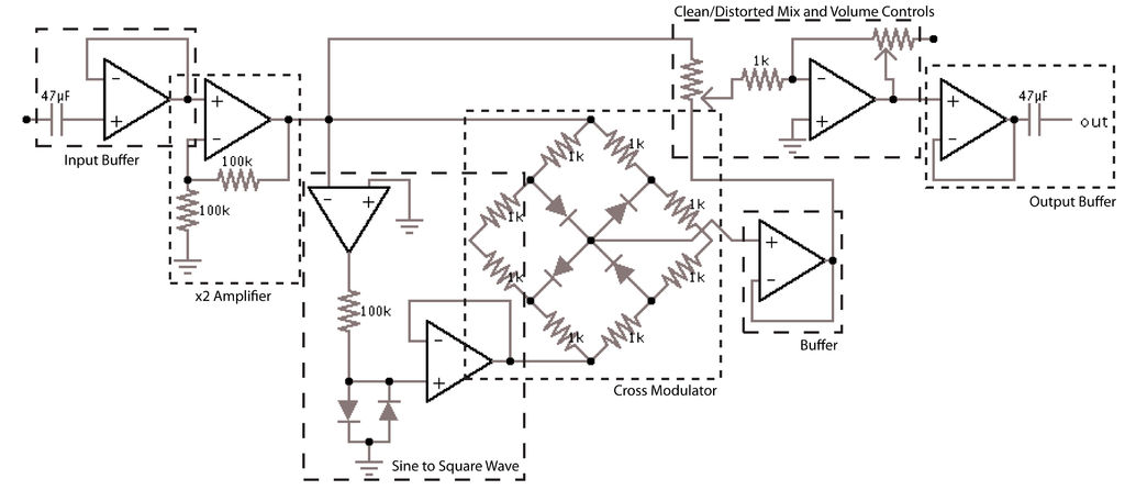 Step 1: Parts Picture of Parts Parts: Resistors (1/4W or greater rating will do) 1k (x9) 100k (x3) 10k linear potentiometer (x1) 10k audio logarithmic potentiometer (x1) Capacitors (16V or greater rating) 47uF (x2) Op Amps TL074 (quad package, x2) 14-pin DIP op-amp sockets (x2) Diodes 1N914 (x6) Other Wire for connections +/-9V power supply (for this project I used the bipolar power supply circuit from geofex.com - http://www.geofex.com/circuits/+9_to_-9.htm) 1/4" mono jacks (x2, input and output) Printed circuit board, bread board, or perforated board The schematic is shown above... Step 2: Theory! Picture of Theory! Waveform.jpg Because who doesn't love to know whats actually going on?! This circuit can be broken down into seven basic pieces, as shown in the first image... The first stage, the input buffer, ensures a high input impedance for the circuit to avoid any signal degradation. The first capacitor blocks any incoming DC offset in the signal, and the value of that capacitor was chosen to make sure that the bass guitar frequency range passes through unaffected. The second stage, the x2 amplifier, is a simple non-inverting amplifier that doubles the amplitude of the input signal. The output from this amplifier is sent to three of the subsequent stages. The Sine to Square Wave step takes the output (which is a superposition of sine waves) from the x2 amplifier and turns the signal into a square wave with the same base frequency as the original signal. It does this by first sending the signal into an op amp set up as a comparator; because the signal is going into the negative input, when the signal has a positive voltage the op amp outputs its maximum negative supply voltage and when the signal has a negative voltage the op amp outputs its maximum positive supply voltage. We thereby get a time-varying output voltage that switches between +9V and -9V (the supply voltages for the op amps). The 100k resistor serves to limit current draw from the comparator op amp. The diodes then clip the square to between ~ +/-1V. This limited square wave is then sent through another buffer to ensure that the signal does not sag. The square wave and the original signal coming out of the x2 Amplifier stage are then both fed into the Cross Modulator*. This part of the circuit multiplies the two input signals together (multiplies them in the time domain, or convolutes them in the frequency domain) to produce strange waveforms, as can be seen in the second image (this circuit simulation and the schematics were created in the incredibly awesome Falstad Analog Circuit Simulator applet, http://www.falstad.com/mathphysics.html). The resulting signal is then fed into another buffer to ensure that the signal does not sag. This crazy signal and the original signal (from the x2 Amplifier) are then combined via a potentiometer (the 'Mix' control) and sent into an output amplifier (whose output volume is controlled with the 'Volume' potentiometer). The final signal is sent into an output buffer to ensure low output impedance and then passed through a final DC blocking capacitor before being sent to the output jack. *The Cross Modulator circuit came from "Comparison of transformerless ring modulators and cross modulators" by Zdenek Mack, published in The Radio and Electronics Engineer, vol. 44, no. 8, August 1974 Step 3: Assembling the Circuit Picture of Assembling the Circuit XMOD_PCB_+parts.jpg TL074 Pin-out.jpg A printed circuit board layout is provided below; the file is designed to be 100% size when printed on an 8.5"x11" piece of paper. A parts layout on the PCB is also provided here. Note that assembling this circuit on the provided PCB will require several jumper wires on the board (shown in the images). These jumper wires are shown as blue lines in the PCB parts layout image. If you use the PCB layout, there is one pad that is supposed to have two wires soldered to it; note in the image of my circuit board that I soldered one of the wires to the pad and then the other wire onto that wire from the top of the board. The large rectangles with the three offset connections on the PCB are for the two potentiometer connections. The wiper (center pin) is connected to the center pad in these sets of solder pads. Note that on potentiometer does not require a connection from one of the outer pins. You can also assemble to circuit on a bread board or on a perforated circuit board with the schematic in step 1. If you use electrolytic capacitors, the negative side should face down-circuit; that is, at the input end, the + side of the capacitor is connected to the signal source and the - side of the capacitor is connected to the rest of the circuit (you can see this in the image of my circuit board - the gray part of the capacitor is the negative side). At the output end, the + side of the capacitor is connected to the circuit and the - side is connected to the output (again, visible in the picture of my circuit board, gray is negative side). I highly recommend you use op amp sockets in assembling this circuit; when you put the op amps into the sockets in this PCB, the markers should be facing away from the 1k resistor. The pin-out diagram for the TL074 chips is also shown here for your convenience... |
«
Return to Requests
|
1 view|%1 views
| Free forum by Nabble | Edit this page |