NPN and PNP Germanium Buffers

classic Classic list List threaded Threaded
16 messages Options
Reply | Threaded
Open this post in threaded view
|

NPN and PNP Germanium Buffers

rocket88
Administrator
This post was updated on .
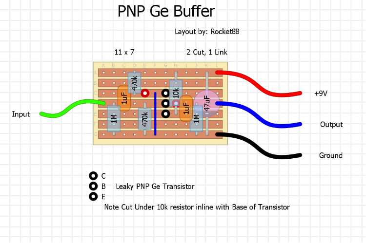
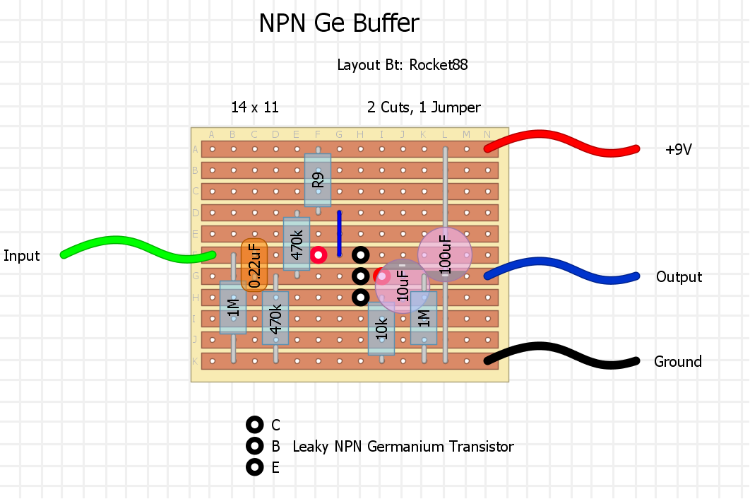
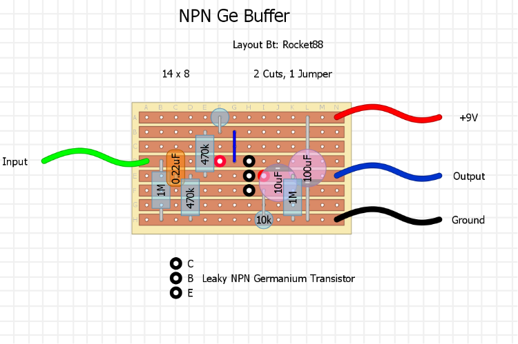
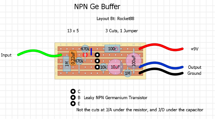
i was thinking that since there are a few of us that have a bunch of Germanium transistors that may be too leaky to be used for a circuit like a FuzzFace, that it might be a good addition to have a layout for both NPN and PNP transistors. I decided to try to do it myself so here is the layout for the PNP Buffer.

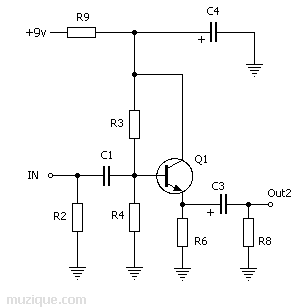
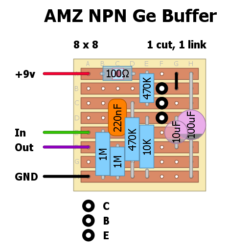
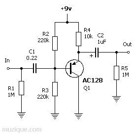
Here's the AMZ Germanium Transistor Buffer Schematic I used to make the layouts, as well as Mark's Tagboard layout on the site for some value changes (the 2 470k resistors in the layout are 220k in the schematic, and the .22uF input cap is 1uF in the layout).


Ge PNP Buffer Without Standup Resistors


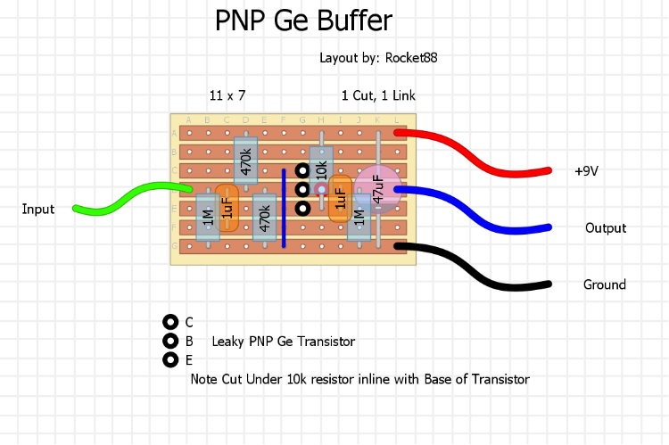
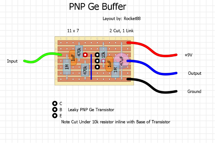
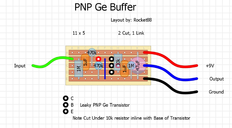
Ge PNP Buffer With Standup Resistors


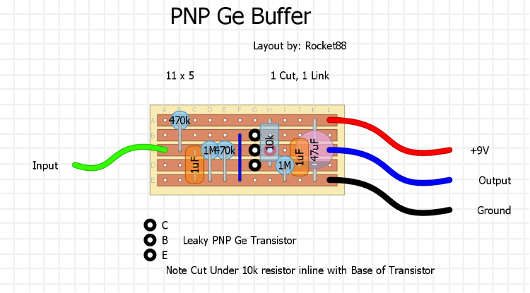
Tried to make it as small as possible, but it only saved 2 rows, so its not a huge difference.
 Btw, this is really the first layout I've made from a using a schematic myself, so go easy on me.
This is not verified yet, so if someone takes a look, I will make the corrections.
Reply | Threaded
Open this post in threaded view
|

Re: NPN and PNP Germanium Buffers

IvIark
Administrator
The input wire, one side of the input cap, one side of the 3 resistors and the base are all connected to the same row without cuts and so all connected.  So a few things need shifting about.
Reply | Threaded
Open this post in threaded view
|

Re: NPN and PNP Germanium Buffers

rocket88
Administrator
I think I see what I did wrong, and had the input cap grounded with the 3 resistors. I think I got it right this time. How does it look now?

Ge PNP Buffer No Standup V2


Ge PNP Buffer Standup V2
Reply | Threaded
Open this post in threaded view
|

Re: NPN and PNP Germanium Buffers

IvIark
Administrator
Not quite.  Put the input wire at the other side of the cap.  Move the bottom lead of the 470K on column D one row lower so it is on the same row as the base.  Move the top lead of the 1M on column B up one row so it's on the same row as the newly placed input wire.  Move the top lead of the 1M on column I one row higher so it's on the same row as the output wire.
Reply | Threaded
Open this post in threaded view
|

Re: NPN and PNP Germanium Buffers

rocket88
Administrator
Damn, I thought I got it right. I tried to think about it as if it should look like the schematic and imagine that there is a single line (wire) that should pass through each component. So I tried to make each component appear in the same order as they appear in the schematic. Mark Can you give me some insight as to why those changes need to be made, so that I can understand it better and hopefully contribute more. FYI, the correct layout as per Marks corrections are below.

Ge PNP Buffer No Standup V3


Ge PNP Buffer Standup V3
Reply | Threaded
Open this post in threaded view
|

Re: NPN and PNP Germanium Buffers

IvIark
Administrator
This post was updated on .
Basically one rule you can never forget is that no two lead component can be mounted horizontally on the same row unless you put a cut in between the leads.  There has to be separation between the two leads of the passive components, if you have them connected on the same row the signal will just bypass them entirely.  So the input connects to one end of the capacitor, and the other end of the capacitor connects to the row that the base is on.

The best way to look at the schematic when converting it to a layout is to concentrate on the points of connection rather than the components.  So looking at the input you can see there are two components at that point, one end of the 220n cap and one end of a 1M resistor.  Then at the next point along you can see 4 connections need to be made, the other end of the 220n cap, one end of two 220K resistors and the base of the transistor.  And that's the way I work through it.  Every time making sure the only components connected at that point are the parts I can see at that point of the schematic.  

I don't know if that makes sense but it's the way I follow it in my head.  Then after a while you just know automatically where things are going to connect a lot of the time.
Reply | Threaded
Open this post in threaded view
|

Re: NPN and PNP Germanium Buffers

Silver Blues
In reply to this post by rocket88
Here's another. If you omit the filter cap there aren't any cuts at all.

Through all the worry and pain we move on
Reply | Threaded
Open this post in threaded view
|

Re: NPN and PNP Germanium Buffers

rocket88
Administrator
In reply to this post by IvIark
AHHH!!! I get it!!! That makes so much sense. The way I had it the input basically went directly into the Base of the transistor, which bypassed the all the passive components along the way, rather then having to travel on each one leading up to the Base like a road. So, I basically created a shortcut through peoples yards.

Thanks Mark. Now hopefully I'll be able to make some more positive contributions.
Reply | Threaded
Open this post in threaded view
|

Re: NPN and PNP Germanium Buffers

Silver Blues
rocket88 wrote
 So, I basically created a shortcut through peoples yards.
bahaha yes. But no, you've got it, I think. I believe your last layout was correct anyway, this was just a simple enough circuit that I thought I'd give you another quick example.
Through all the worry and pain we move on
Reply | Threaded
Open this post in threaded view
|

Re: NPN and PNP Germanium Buffers

rocket88
Administrator
Hey I just had to come up with some strange analogy to help me better think about it. I felt confident enough to try to build an NPN buffer based on the AMZ NPN Ge Buffer.


Values on Schematic
R2 - 1M
R3 - 470k
R4 - 470k
R6 - 10k
R8 - 1M
R9 - 100 ohms
C1 - 0.22uF
C3 - 10uF
C4 - 100uF
Q1 - NPN germanium transistor

Here are my layouts:

Without Standing Resistors


With Standing Resistors


Hoping for a thumbs up on the first try on this one.
Reply | Threaded
Open this post in threaded view
|

Re: NPN and PNP Germanium Buffers

Heath
Here's my version, Rocket.  I wouldn't mind making a few of these and I'm still learning, so I figured I'd try my hand at this circuit as well since it's low parts count.  The thing I hate about building buffers is it's hard to hear if they are working without some effort (unless you guys have some sort of neat trick to verify such).  Here's what I came up with so far:


I cheated a little bit with the 3 hole span resistors, but when I have one next to the edge, I can easily hang it's little butt off the side a little bit without it standing.

Of course I might have just horked it up big time.  
Reply | Threaded
Open this post in threaded view
|

Re: NPN and PNP Germanium Buffers

IvIark
Administrator
In reply to this post by rocket88
Yes this one is looking good to me.  So once you have the layout correct just look at it and see if there is anything obvious you can do to make it better.  To me there is one obvious thing that you could do to make it a little more compact.  The second and third rows from the bottom are currently completely unused, so instead of taking R9 up and needing an extra 3 rows at the top, bring it down to the second from bottom row (move the blue link a couple of columns to the right if you need to).  This gives you an additional advantage because now your power supply filter cap only has to go from the bottom to the second from bottom row, so you don't need to span the whole board with a radial component.

rocket88 wrote
Reply | Threaded
Open this post in threaded view
|

Re: NPN and PNP Germanium Buffers

IvIark
Administrator
In reply to this post by Heath
This one looks good too buddy, nice and compact.  I will avoid 3 hole span resistors if I can, but I will include them most of the time if the only other option is to add an extra row.  I got a set of 1/8W resistors specifically for this which will lie flat with a 3 hole span.

Heath wrote
Reply | Threaded
Open this post in threaded view
|

Re: NPN and PNP Germanium Buffers

rocket88
Administrator
This post was updated on .
Awesome. I made mine bigger to make sure that the resistors didn't span more then 4 rows so they lay flat. I'm going to see how much smaller I can make mine so that I can fit it into a tiny 1590A. I'm glad that it's sinking in and making sense.  thanks for the guidance Mark.

Here's V2 for the NPN Ge Buffer, if you don't mind standing resistors.


It's a little longer then I want, but its only 5 rows wide, so I'm pretty pleased.
Reply | Threaded
Open this post in threaded view
|

Re: NPN and PNP Germanium Buffers

Heath
Hey, Rocket, thanks for inspiring me to give this one a shot.  Thanks, Mark for the feedback and encouragement.  Definitely something neat to do with the weaklings of the Ge bunch.
Reply | Threaded
Open this post in threaded view
|

Re: NPN and PNP Germanium Buffers

rocket88
Administrator