Phase Shift Switch
|
I am interested in adding a 180 degree phase shift switch to each of the sends of this JFET parallel looper. I've found a phase shifter schematic to do this but as a beginner in electronics I'm not at a point yet where I can add this to a stripboard layout on my own. Perhaps there is a simpler way to do this I'm not aware of? I also found this DPDT phase reversal switch for pickups but I'm not sure if it can or how it would be used for this particular application. Can someone please assist me in either adding phase shift switches to the looper layout or a daughterboard version that could easily be added to each send? Your help is appreciated!!!
|
|
Would the buffer/phase inverter one here work? If so, how would I omit the buffer and only keep the phase inversion?
|
|
Yes, the buffer/phase inverter one should work fine. It's pretty much the same circuit as the schematic you linked to, with an added input buffer to overcome the inverting op amp's somewhat low input impedance. You shouldn't remove the buffer, it's needed for the phase inverter. If you want your non-inverted signal to be unbuffered, just wire the circuit like a pedal and bypass it entirely when you aren't using it.
Be aware that the inverted signal will be buffered, though, so the tone might not be consistent in bypass. Generally speaking, your ear cannot detect phase inversion by itself, so listen to it without anything else in parallel. If you hear a difference between the true bypassed signal and the inverted one, that's the effect of the buffer. The DPDT version won't work (pickups don't care which wire is attached to ground, pedals do). |
|
Thanks induction!
With that information I should be able to get this part working pretty easily. I'm wanting to put this in a 1032L enclosure with both series and parallel loops available so I'm hopeful that space for these daughterboards shouldn't be too big of an issue. How would I go about adding stomp switches to each channel of the parallel looper? Is this feasible? If not I can probably do without them but it would be nice to be able to bypass each channel separately. |
|
A simple SPST on the signal line for each send should work. You can wire the ground directly to the jacks without a switch. The looper has pulldown resistors on the sends, so it shouldn't pop, but no guarantees.
|
|
That would be a simpler solution and if it's more hassle than it's worth I just might do that but I'd like to use stomp switches and have led indicators for each channel's on/off state.
|
|
Sure, that's what I figured. But I'll be more explicit.
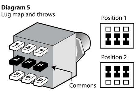
 1. Use the 1st pole of the stomp switch (lugs 1, 2, 3) as an SPST for the signal wire. Connect lug 1 to the signal wire and lug 2 to the jack. Leave lug 3 disconnected. 2. Use the 2nd pole (lugs 4, 5, 6) as an SPST for the led. Led anode on lug 4, ground on lug 5. Leave lug 6 disconnected. CLR between led cathode and V+. You can use a 2PDT switch for this if you have one (they generally have softer touch than 3PDTs, so some people prefer them), or use a 3PDT and ignore the 3rd pole (lugs 7, 8, 9). Looking at the schematic, I would put the phase inverter switch after the on/off switch to avoid popping. If you put it in front, add an output cap and a pulldown resistor to the phase inverter output (100n and 1M should work). Finally, I'll note that the phase inverter layout doesn't include any power filtering. The circuit is low-gain, so it shouldn't be too bad, but I'd add a low-pass on the power rail anyway. 100R and 100u is a good combination. |
|
This post was updated on .
Thanks again, that was tremendously helpful to my understanding of switches. I have some 2PDT switches as well so I will use those. I may have to experiment a bit to understand what you mean about the power filtering as that is not something I've explored yet. I would assume that I would need to expand the layout to 12x10 and then the 100R resister connects the power rail to the positive side of the 100u capacitor(if using electrolytic) and the negative side to ground. Is this correct or is there more to it? Picture of modified circuit added for illustration. Edit: Incorrect layout redacted, see corrected layout below. |
|
This post was updated on .
That's pretty close.
Here's what a low pass filter looks like:  The filtered V+ comes from the junction between the resistor and the cap. That's what you want to feed to the rest of the circuit. So here's what I would do, starting with your modified layout: 1. Move the cut and link in column J to column H, same rows 2. Move the 100R from column K to column J, same rows 3. Move the 100u from column L to column K, negative leg on row J, positive leg on row C 4. Move the V+ input to row I, all the way on the right |
|
This post was updated on .
I've modified the layout with your suggested changes and added labels, does this look correct? Edit: Incorrect Layout Redacted, see corrected layout below. |
|
Sorry. The positive leg of the 100u should be on row C, not D. My fault. (I edited my previous post to avoid confusion.)
Looks good otherwise. |
 Fixed! Thanks again for your help! I will be building this very soon! |
| Free forum by Nabble | Edit this page |

