hey, thanks for your answer!
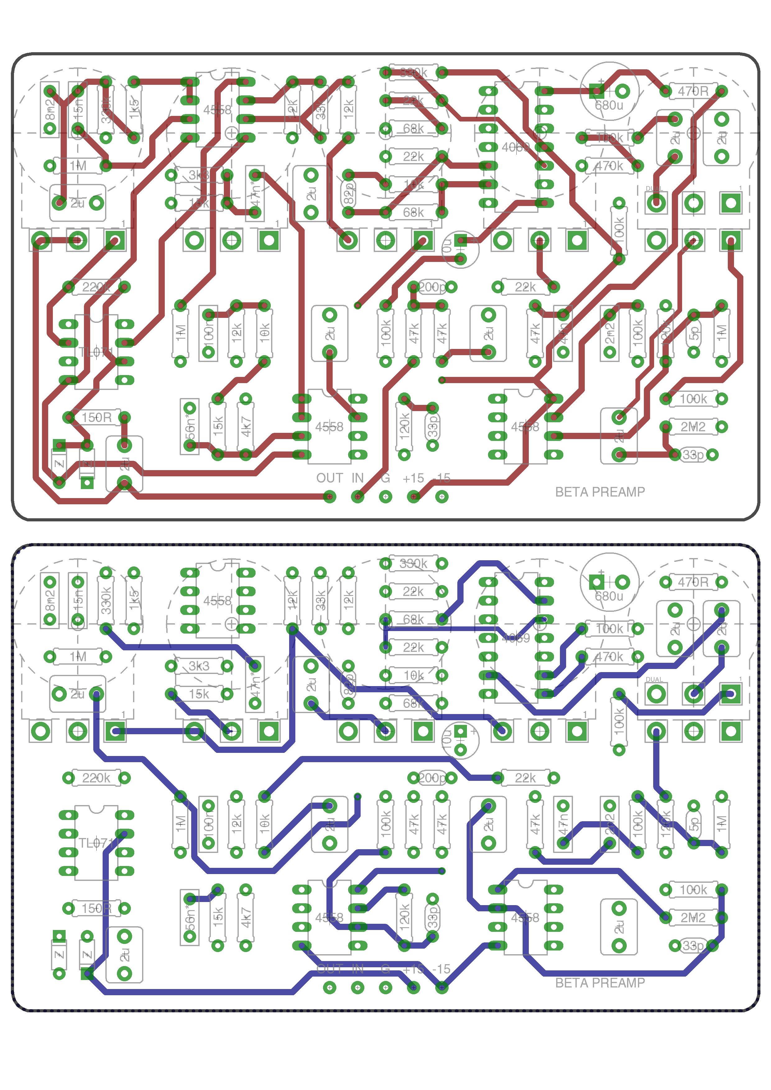
i'm assuming, it's something like this...
i'm using a ground plane on my bottom layer only, used Eagle for this.
here's a print file for top (red) and bottom (blue) layer (without the ground plane, though).

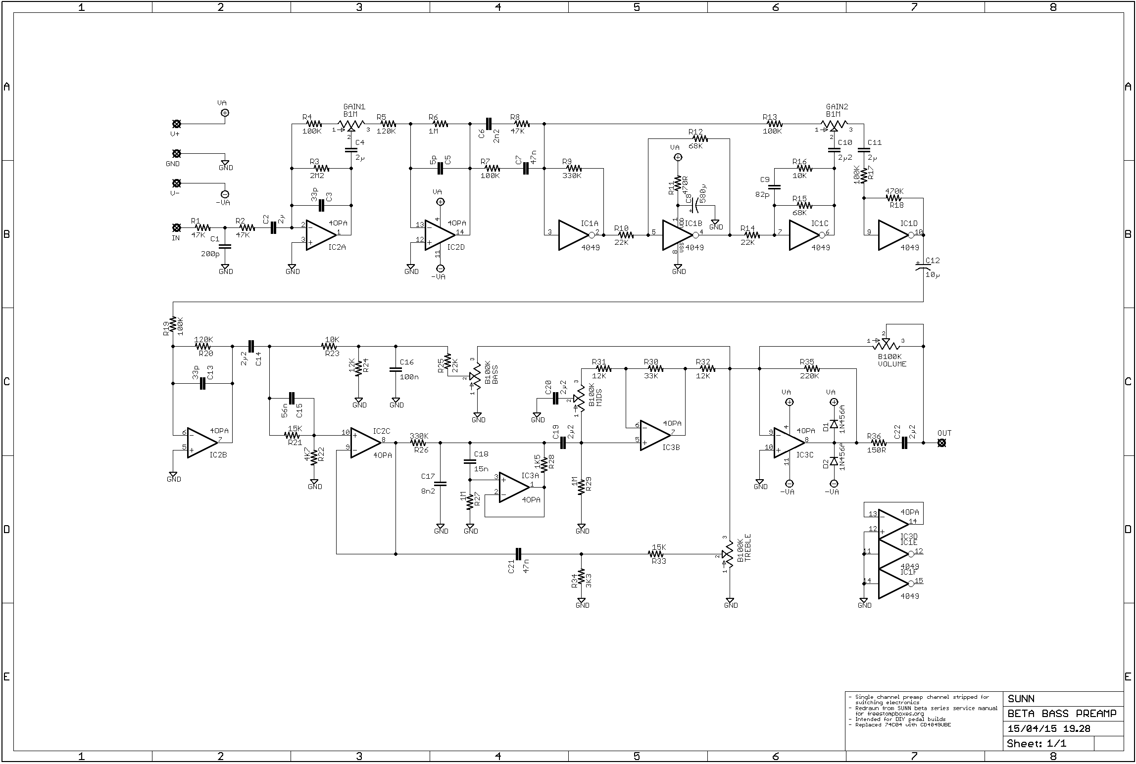
and here's the schematic I've used (using a 4069 instead of a 4049, so the pinout is different).

I can't be 100% sure layout vs schematic is ok, but honestly, I've checked it so many times...
If we're talking about traces too close, the traces between the 4069 pads on the bottom layer are quite suspicious :D
If you have any advice/resource on "how to route a pedal PCB properly", I would be quite grateful!!!
thanks in advance!