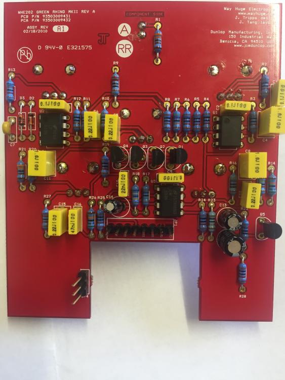
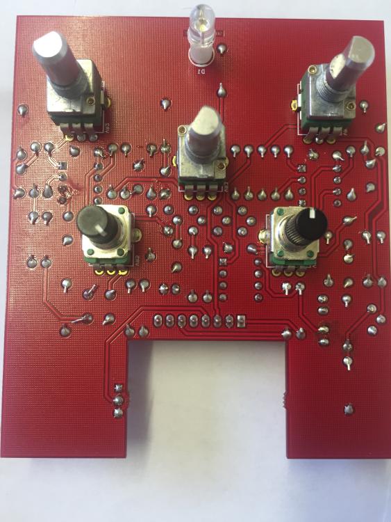
One of our students had this in today and allowed me to take it apart and see what's going on for a few hours. And sure enough it's YATS (as we knew from MK1) with a few mods and something I'm hoping someone can enlighten me on.
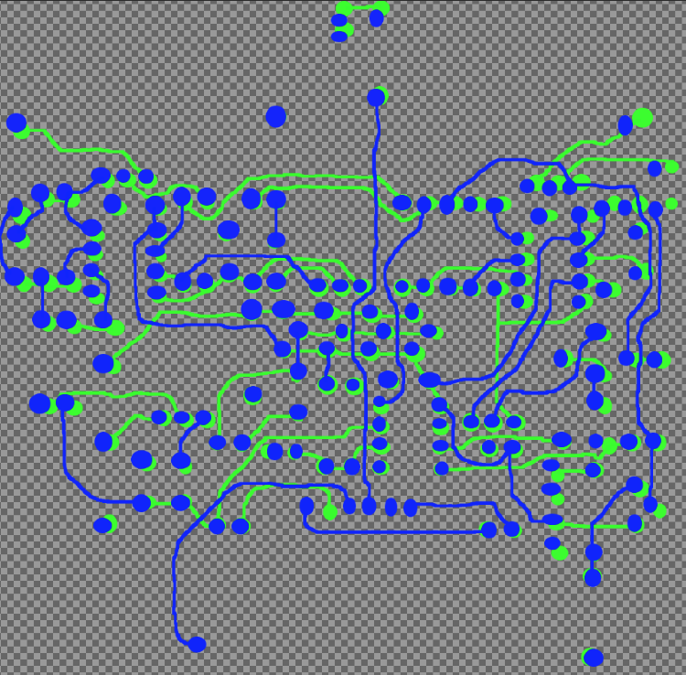
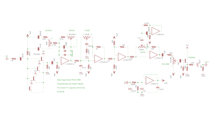
Some pics for whoever wants to cross reference the schematic with.


I missed the 10u>10K>GND trace on this pic but it's all fine on the schematic AND apologies for not lining up the front/reverse pics better before I started. I had little time.
The Schematic (massively overcomplicated relay switching omitted

)and hi res
here
So my question...what is the point of 4 BJT in parallel at the input buffer? This wrecked my head for way longer than it should! I initially thought there was some kind of design error....or I missed some traces but nope...4 transistors in parallel acting as nothing more than a buffer. Anyone know why they couldn't just use 1 like any other TS?
Anyone want to tackle a breadboard/layout and make an eejit out of me?

I should point out that another forum member also had a go at tracing this
here but I'm very confident there are a few errors. Still...it's good for referencing anyhow.
Cheers folks...hope all turns out well