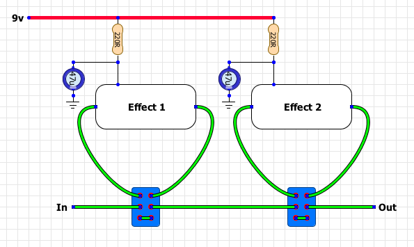
The path would go:
Input jack -> switch 1 input (wire effect number 1 with true bypass)
then
switch 1 output -> switch 2 input (wire effect number 2 with true bypass)
and finally
switch 2 output -> output jack
Power wise, run the 9v into a low value resistor (ie 100/220R) and then put a high value electrolytic to ground. Do this for each board.
Here's a quick sketched schem/layout hybrid thing I made...

That's how I would do it anyway, if anyone has a better way of doing it (or explaining/illustrating it...!) I'd love to hear, I have a predrilled triple enclosure waiting on my desk, will probaby go for a OD->Fuzz->Delay combo...!
Hope this is clear enough and of any help!