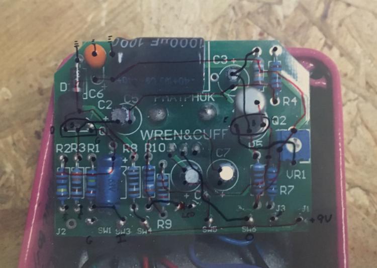
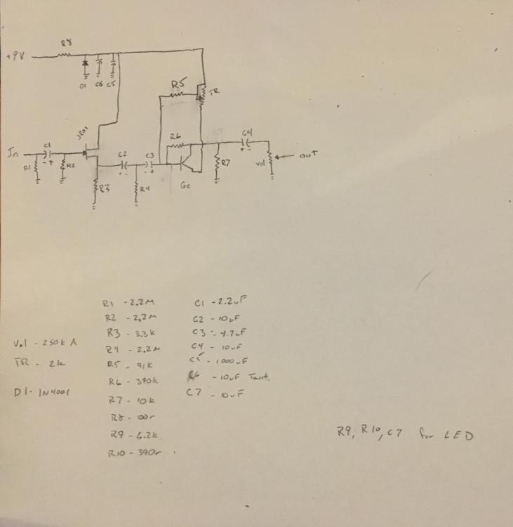
so i posted a request for this a long time ago, but i actually got my hands on one and traced it. i posted a layout for it on the main page, but figured i would post up some pictures of the board front and back, my trace, and the schematic so that it can be looked over to make sure i've got it right.
Front:
<nabble_img src="photo_1.jpg" border="0
Back:
<nabble_img src="photo_2.jpg" border="0"/>
Trace:

Schematic:

a couple of notes:
1 - there are a few tracts hidden by components, which i figured out by placing a light behind the board, and carefully moving some of the components out of the way.
2 - the Ge transistor has its markings removed, as well as the FET being sanded down. the only markings that can be seen on the Ge is what looks like AX9 which matches up to Chinese Ge transistors, but i do not know if it's PNP or NPN, and the FET is clearly a J201.
3 - the FET buffer makes sense to me, but the Ge section just seems really odd, and doesn't resemble a booster or buffer that i've ever seen before. which is why i figured it would be a good idea to have others look over the trace and schematic.
4 - the build quality is incredibly disappointing. the soldering is shit, the board is very low quality making it hard to remove components which is why i didn't/couldn't, and the wire is complete garbage with each one breaking at least ones while moving the board around. honestly incredibly disappointing coming from a "boutique" company, and all everyone here should be incredibly proud of the quality of all your builds.