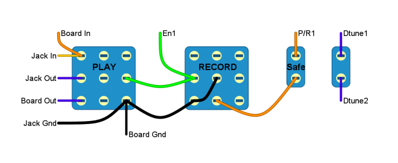
Checking the layout he's changed the labels on the diodes from the schematic. Mine should be right. D1=1N4001, D2,D3 = 1N914. Sorry I didn't check his pcb layout when I did mine so missed the switches. Check the switching below I think it's ok - just disregard the En2 and Safe2 grounding on the board layout and the P/R2 - Safe 1.

Why the 3PDT's? Perhaps use the unused sides for LEDs?