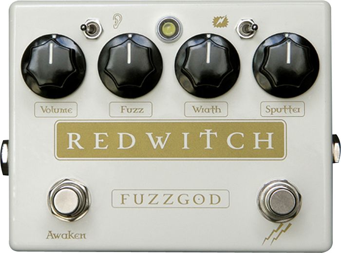
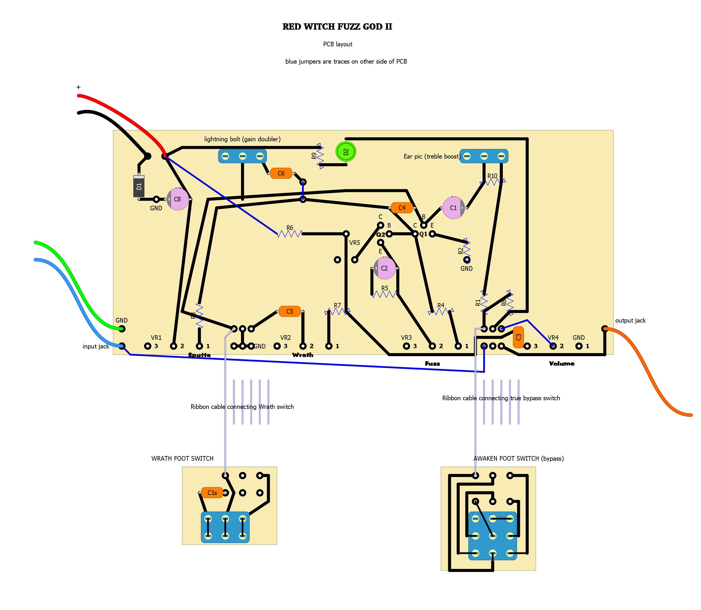
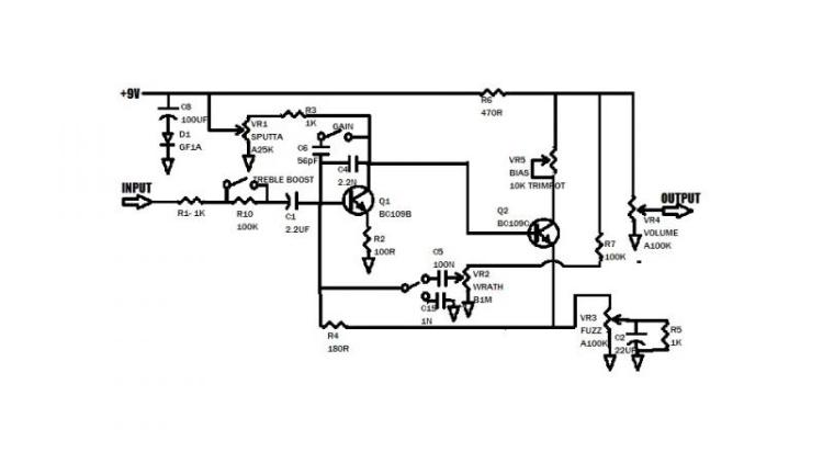
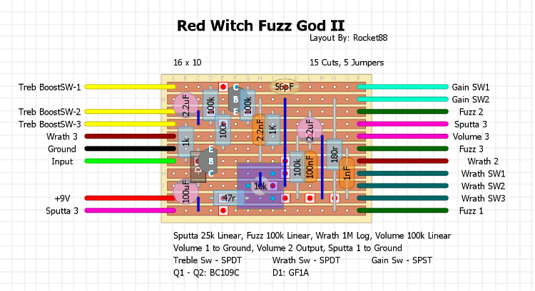
RED WITCH FUZZ GOD II PCB layout

1234

1234
RED WITCH FUZZ GOD II PCB layout

|
Re: RED WITCH FUZZ GOD II PCB layout
|
|
Re: RED WITCH FUZZ GOD II PCB layout
|
|
Re: RED WITCH FUZZ GOD II PCB layout
|
Administrator
|

Re: RED WITCH FUZZ GOD II PCB layout
|
Administrator
|

Re: RED WITCH FUZZ GOD II PCB layout
|
|
Re: RED WITCH FUZZ GOD II PCB layout
|
Administrator
|
Re: RED WITCH FUZZ GOD II PCB layout
|
|
Re: RED WITCH FUZZ GOD II PCB layout
|
|
Re: RED WITCH FUZZ GOD II PCB layout
|
|
Re: RED WITCH FUZZ GOD II PCB layout
|
|
Re: RED WITCH FUZZ GOD II PCB layout
|
|
Re: RED WITCH FUZZ GOD II PCB layout
|
Administrator
|
Re: RED WITCH FUZZ GOD II PCB layout
|
|
Re: RED WITCH FUZZ GOD II PCB layout
|
|
Re: RED WITCH FUZZ GOD II PCB layout
|
|
Re: RED WITCH FUZZ GOD II PCB layout
|
|
Re: RED WITCH FUZZ GOD II PCB layout
|
Administrator
|
Re: RED WITCH FUZZ GOD II PCB layout
|
|
Re: RED WITCH FUZZ GOD II PCB layout
|
Administrator
|
| Free forum by Nabble | Edit this page |